TLMBoy: The CPU
1. Introduction
This is another post of my TLMBoy series which revolves around writing a Game Boy Emulator using SystemC TLM-2.0. In particular, the following sections cover the structure and implementation of the Game Boy’s CPU. Without further ado, let’s get right into it!
In the heart of every compute system you will probably find a CPU (Central Processing Unit). Or today it would be more like multiple CPUs, but in the case of the Game Boy, it’s only one Sharp SM83. Its job is quite simple: execute the instructions from your cartridge. Each of the instructions does a small part, like adding two numbers or moving some data from A to B, but the symphony of thousands of them can create the impression of an italian plumber eating mushrooms. While there are also some other components involved in this process, like the PPU (Pixel Processing Unit), the APU (Audio Processing Unit), or the Joypad, it is the CPU that orchestrates them.
In the following, I’ll first provide you with a general workflow of the SM83 and then highlight certain aspects
like the register file.
Since I mainly focus on coding, most sections comprise some code snippets, including some thoughts about the particular design.
If you’d like to see the whole code, feel free to pay my GitHub repository a visit (especially cpu.h, cpu.cpp, cpu_jumptable.cpp, and cpu_ops.cpp).
2. CPU work flow
As already mentioned before, executing instruction is one of the CPU’s main tasks. These instructions are found in binary form in the cartridge and are loaded/executed by the CPU. For most CPUs the process from load to execution can be divided into several single stages. The Game Boy’s SM83 stages are depicted in the following, simplifying graphic.

Seperating the instruction execution into multiple stages isn’t only advantageous from the comprehension perspective. In fact, it’s also how it’s really implemented! With each clock cycle instructions are usually forwarded from one stage to the next one. So, looking at graphic above, some interesting questions may arise:
- The most obvious ones: What are the stages actually doing?
- But also: How long does it take for an instruction to be executed?
- Or: How many instructions can the CPU execute in a given time frame?
The former question takes a few words to answer, so let’s quickly focus on the last two. From the graphic above, one might assume that an instruction takes 2 cycles to be completed. In the fist cycle it’s fetched from the cartridge and decoded, while in the second it is executed. This is true for many instructions, but there are also quite a few instructions that reside up to 3 cycles in the decode and execute stage. Hence, an instruction requires between 2 and 4 cycles to be executed. Would this now mean that the CPU completes between 0.5 and 0.25 instructions per cycle?
Interestingly, the answer to this question is “no” as a technique called pipelining is employed by the SM83.
With this enhacement multiple instructions ripple through the two stages at the same time!
This is pretty much like doing laundry.
If your washing machine is finished, you can put your clean clothes into the dryer and start another round of washing at the same time.
While this analogy might seem odd at first, it describes the situation quite accurate!
Assuming that each instruction takes 2 cycles to finish, the CPU can finish up to one instruction in one cycle in case the pipeline is filled. But what about instructions that reside multiple cycles in the last stage? Or in terms of our analogy: What if the dryer takes longer than washing?
Well, they just let the preceding instruction/stage wait.
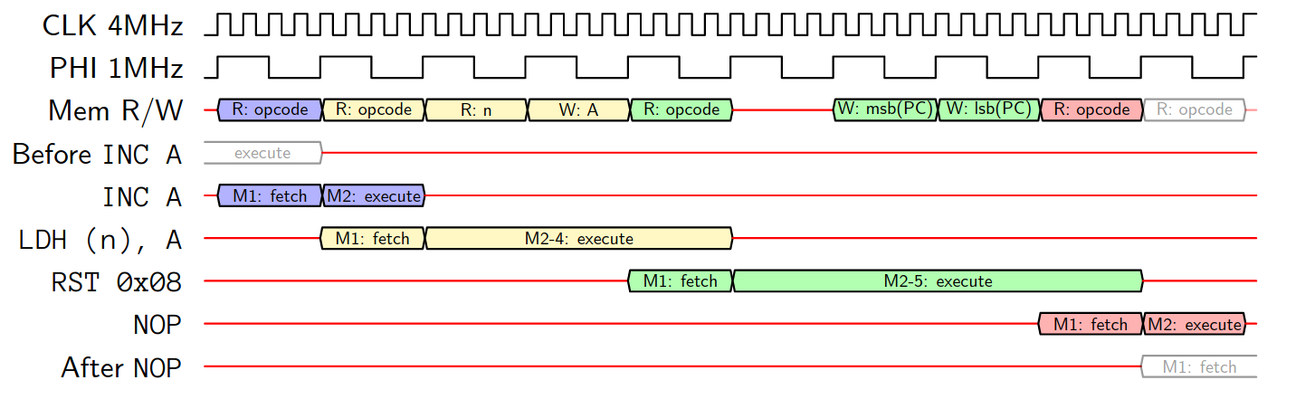
The following graphic I found in [1] visualizes this quite well.
For instance, you can see that the INC Ainstruction is still being executed while the next instruction LDH (n), A is already fetched:
So, that was a lot information, but the good message is: It is possible to simplify the model quite signficantly! Because emulation usually also means simplification. We’re just interested in the correct in-/output behaviour of a system, not in the way how it actually achieves this. In case of a Game Boy emulator we can assume a so called Simple Sequential Execution (SSE) model. The idea behind this model is quite straightforward. We just execute everything from fetch to execute in virtually zero time. Afterwards the CPU waits for an instruction-dependent time which is derived from a fully utilized pipeline. Ok, you might say, but isn’t this inaccurate? To a certain extend yes, but altering the timing does usually not affect the functionality. Hence it is good enough to emulate most of the games :)
2.1 Fetch
As shown above, the CPU starts with the fetch stage in order to obtain an instruction. For this, the byte that is addressed by the PC (program counter) register is loaded from the memory. However, the Game Boy has variable length instructions with some of them requiring up to 16 bits. In this case the fetch acts accordingly and loads two bytes.
Since you usually want to execute the next instruction after an instruction, the PC register is automatically incremented by 1 or 2 after the fetch. There are a few exceptions like jump instructions, but more about that later.
So assuming the next instruction is 1 byte instruction.
The correponding code can be found below in the Cpu::FetchNextInstrByte() function and looks like this:
u8 Cpu::FetchNextInstrByte() {
  u8 val = ReadBus(reg_file.PC);
  ++reg_file.PC;
  return val;
}
2.2 Decode
After fetching the data, the CPU interprets it as an instruction and executes it. Interestingly, the CPU does not distinguish between instruction data or other kinds of data. This means, if you make a few mistakes when programming a Game Boy game, it could happen that image data can also be executed as instructions, which probably leads to odd behavior. However, players can exploit these bugs to achieve even faster speedruns (glitching) or clone a bunch of master balls. An interesting part of programming an emulator is finding an efficient and clean way to decode the instructions.
A pretty straight-forward approach are jump tables.
These tables map each possible instruction byte to a certain instruction.
In C++ this corresponds to simple switch/case statements as show in my code below.
This method is quite performant if your compiler optimized properly (O(1) in theory),
but you might run into some problems depending on your architecture.
The Game Boy supports roughly 500 instructions which is still manageable with switch/case statements.
Modern architectures, like Armv8-A, have a 32-bit instruction width resulting in more than 4 billion possibilites.
Good luck with typing them all in a jump table!
Very similar to jump tables are function arrays. Here, the correct instruction is chosen by using the instruction byte as an index for an array of function pointers. Again the decoding time is a O(1), but in contrast to jump tables, you don’t rely on the compiler’s optimizations. Also similar to jump tables, the array grows exponentially with the number of instruction bits.
As a solution to the growing number case-statements/function array entries, you can try to exploit the inherent structure of the instructions. Usually instructions are built up in a very systematic way. Like the first 4 bits describing your operator (e.g. addition), the next 5 bits your first operand (e.g. register 1), and so forth. So, as an alternative can you try to write decoder that tries to determine operands and operators depending on certain bits in the instruction.
To give you a better feeling of the decoder implementation, I assembled a list with various Game Boy emulators and their decoder type.
| Emulator | Decoder Type | Code Reference |
|---|---|---|
| binjgb | Jump Table | source |
| Dromaius | Jump Table | source |
| GBEmu | Decoder | source |
| gbemu | Jump Table | source |
| Gearboy | Function Array | source |
| PatBoy | Function Array | source |
| PyBoy | Jump Table | source |
| SameBoy | Function Array | source |
| Visual Boy Advance | Jump Table | source |
| xgbcdyna | DBT | source |
As you can see, the prevailing methods are jump tables and function arrays. I only found one emulator using a decoder. The reason for this might be the odd instruction encoding of the Game Boy which doesn’t make decoders very appealing. If you want to go above and beyond in terms of performance, you could also use a technique called dynamic binary translation (DBT). With this method you dynamically recompile the Game Boy’s machine code into your host’s systems architecture. Sounds simple, but is by far the most complicated solution.
In the end, I implemented a jumptable decoder for the TLMBoy. A corresponding code snippet can be found below. To link the cases with their corresponding instructions, I used this resource.
As you can see in the link and in my code snippet, one last corner cases needs to be considered: the variable instruction width. This means, a Game Boy instruction can be either 8 bit or 16 bit! If the first fetched byte is a 0xCB, the Game Boy fetches another byte which is interpreted differently. Incorporating this in a jumptable is straight forward: just nest another jumptable!
void Cpu::EvalInstr() {
  // Fetch.
  u8 instr_byte = FetchNextInstrByte();

  // Decode & execute.
  switch (instr_byte) {
    case 0x00:
      DBG_LOG_INST("NOP");
      InstrNop();
      break;
    case 0x01:
      DBG_LOG_INST("LD BC,u16");
      InstrLoadImm(reg_file.BC);
      break;
      ...
    case 0xCB:  // special bit instruction is called
      instr_byte = FetchNextInstrByte();
      switch (instr_byte) {
        case 0x00:
          DBG_LOG_INST("RLC B");
          InstrRlc(reg_file.B);
          break;
    ...
}
2.3 Execute
After the decoding stage, we finally reach the heart of the Game Boy: the execute stage. Here is where the magic happens with the instructions finally taking an effect on the Game Boy’s state. There are quite a few instructions supported by the Game Boy (see [2]) and analyzing them would probably require multiple posts. This is why I first want to give you a rough overview on the structure of instructions which is then followed by a few examples. If you’re looking for the details of a particular instruction, you can either refer to the TLMBoy’s implementation or take a look at the GBCPUMan [3]. Anyway, let’s start at the beginning!
Every processor can be classified according its so called Instruction Set Architecture (ISA). The ISA primarly determines which instructions are supported and to which encoding they are mapped. But also things like the register file size are defined by the ISA. Its purpose is to create a common ground for software workloads, meaning that a given program can be executed by any processor as long as it’s the correct ISA.
In general, ISAs can be divided into two categories: RISC and CISC. CISC ISAs have a variety of supported instructions that are usually quite powerful. This allows you to have descriptive assembly programs in just a few instructions. A characteristic that is quite favourable, if your system doesn’t have a lot of memory, and if you have to program it in asssmbly. As these constraints are particularly true for very old systems, many of them, inlcuding the Game Boy, can be classified as CISC. The advantage of RISC lies in its simple instructions allowing for simpler and faster hardware implementations. From the Emulator perspective we’d favour RISC ISAs as there are less instructions to implement. Besides that, it doesn’t really make a difference implementation-wise. So, now we know that he Game Boy is a CISC ISA, but which one is in particular? The Instruction Set Architecture (ISA) of the Game Boy is more or less a Z80 (link) clone. It’s not exactly
- difference Z80 SM83
- Typical instruction: arithemtic stuff or move data from a to b, also
- Example:
void Cpu::InstrAddA(Reg<u8> ®)This instruction adds the value of another register to Register A. It also sets a bunch of flags. For instance, Z is set, if the result in A is 0. Furthermore, here instructions comprise the timing annotation. simple sequential execution model (SSE) Another example:void Cpu::InstrCall(), which is used to call functions. Prefix-notation is used: first stack pointer is decremented, afterwards its value is stored on the stack. Quite a long timewait(24).
void Cpu::InstrAddA(Reg<u8> ®) {
SetFlagH((reg_file.A & 0x0f) + (reg & 0x0f) > 0x0f);
reg_file.A += reg;
SetFlagN(false);
SetFlagC(reg_file.A < reg);
SetFlagZ(reg_file.A == 0);
wait(4);
}
void Cpu::InstrCall() {
u16 jmp_addr = FetchNext2InstrBytes();
WriteBus(--reg_file.SP, reg_file.PCmsb);
WriteBus(--reg_file.SP, reg_file.PClsb);
reg_file.PC = jmp_addr;
wait(24);
}
3.3 The Register File
 A register file is a scratchpad memory integrated in the CPU that can be used to load and store data.
As the name suggests it comprises multiple so called registers allowing a super fast data access.
In today’s compute systems accessing data from the register file can be 100x faster than accessing it from the RAM!
So why don’t we forego the main memory and only work with these super fast registers?
Well, there are only a few of them available.
In fact, the Game Boy has so few, that they have names:
A register file is a scratchpad memory integrated in the CPU that can be used to load and store data.
As the name suggests it comprises multiple so called registers allowing a super fast data access.
In today’s compute systems accessing data from the register file can be 100x faster than accessing it from the RAM!
So why don’t we forego the main memory and only work with these super fast registers?
Well, there are only a few of them available.
In fact, the Game Boy has so few, that they have names:
A, B, C, D, E, F, H, L, SP, PC.
Most of the registers store results and operands from operations and can freely be used by the programmer.
The registers A, B, C, D, E, F, H, and L are 8 bit wide. That’s why the Game Boy is an 8 bit console!
However, depending on the instruction, the CPU can also interpret some two 8 bit registers as one 16 bit registers.
Possible pairs are: AF, BC, DE, and HL, whereby the first register always denotes the MSB (Most Significant Byte)
The registers SP and PC are 16 bit by default serve a special purpose:
The PC register is the so called program counter. It points to the address of next instruction and is usually automatically incremented when an instruction is executed. Only control flow operations such as jumps or calls directly set the PC to a new value. When you turn on the Game Boy, it’s one of few registers having a guaranteed value which is O in PC’s case.
Kind of related to the PC register is the SP (stack pointer) register.
It points to the last element of the (call) stack which is a dynamic data structure growing downwards in the address space.
The stack can be used for multiple things, but its main purpose is to store old PC values.
A good example for stack usage is a function call.
Calling a function is usually achieved by executing the call <address> instruction.
This instruction pushes the current PC on the stack before jumping to the address of the called function.
By later popping it from the stack (using a ret instruction we can return to the subsequent instructions.
During the boot process SP will be initialized to 0xFFFE from where it will grow downwards to smaller addresses.
Another special register is the F (Flag) register. Here, bit 4-7 indicate special events that might have been triggered by a preceding instruction. The events in particular are:
- Zero Flag (Z) / bit 7: This bit is set if the result of an arithmetic instruction was zero.
- Subtract Flag (N) / bit 6: This bit is set if a subtraction instruction was executed.
- Half Carry Flag (H) / bit 5: This bit is set if there was a carry from the lower nibble.
- Carry Flag (C) / bit 4: This bit is set if there was carry. Refer to the opcode table in case you execatly want to know, which flag is raised by which instruction. Important detail: The lower 4 bits of this register always read as zero (especially important for “POP AF”!
The implementation of the register file is quite straight forward and doesn’t require any SystemC intrinsics.
template<typename T>
class Reg {
  public:
    const std::string name;
    Reg(std::string name, T &value) : name(name), _value(value) {
    }

    T val() {return _value;}
    void val(T val) {_value = val;}
    void valByHexStr(const std::string &r) {
      _value = std::stoi(r, nullptr, 16);
    }

struct RegFile {
  public:
    Reg<uint8_t> A, F, B, C, D, E, H, L, SPmsb, SPlsb, PCmsb, PClsb;
    Reg<uint16_t> AF, BC, DE, HL, SP, PC;
    RegFile() :  A("A", _dat[1]),
                 F("F", _dat[0]),
                 B("B", _dat[3]),
                 C("C", _dat[2]),
                 D("D", _dat[5]),
                 E("E", _dat[4]),
                 H("H", _dat[7]),
                 L("L", _dat[6]),
                 SPmsb("SPmsb", _dat[9]),
                 SPlsb("SPlsb", _dat[8]),
                 PCmsb("PCmsb", _dat[11]),
                 PClsb("PClsb", _dat[10]),
                 AF("AF", reinterpret_cast<uint16_t&>(_dat[0])),
                 BC("BC", reinterpret_cast<uint16_t&>(_dat[2])),
                 DE("DE", reinterpret_cast<uint16_t&>(_dat[4])),
                 HL("HL", reinterpret_cast<uint16_t&>(_dat[6])),
                 SP("SP", reinterpret_cast<uint16_t&>(_dat[8])),
                 PC("SP", reinterpret_cast<uint16_t&>(_dat[10])) {}
  private:
    uint8_t _dat[12];
};
As you can see I started with an implementation of a register class Reg first.
In my case I used a template class to abstract the register from their data type as their can be two kinds of registers: 8 bit and 16 bit. Furthermore, registers also have a string member name representing their… name.
This used later just for convenient purposes.
Note, that registers receive _value as a reference. This makes it possible to have multiple registers working on the same data and will be used to implement fused registers.
In RegFile you can find the actual registers, including their fused versions.
But beware, if you run this on a big endian machine, things might blow up due to _dat array which is reinterpreted as
an unsigned 16 bit register.
Besides that, the Game Boy can also merge some of the 8bit registers into 16bit registers.
To be exact, there is:
AF, BC, DE, and HL.
Instructions
Interrupts
Timer
Summary
| Name | SM83 |
| ISA | Z80/8080 (CISC) |
| Clock Speed | 4.19 MHz / 1.05 MHz |
| Instruction Width | 8 or 16 bits |
| Register File | A,B,C,D,F,H,L,SP,PC |
| Address Width | 16 bit |
| Data Width | 8 bit |
| Pipeline | 2-stage Fetch/Execute |
References
[1] Game Boy: Complete Technical Reference
[2] Game Boy Instruction Table
[3] Game Boy CPU Manual